Python: Analog Inverter Chip Layout with Magic and PySpice Simulation on Sky 130nm PDK
This notebook demo how to create inverter loayout and extract analog net-list to simulate with Sky 130 nm PDK. Assume you are login to any compute node in exascale.mahidol.ac.th AI/HPC cluster.
Considering CHIP, ASIC shortage after Covide-19, Euro WAR and Taiwan-China security and political issue. They are looking for Plan B, alternative CHIP factory. It is not goal to change country business focus but motivation for new generation to want to explore HOW TO BUID REAL CHIP as Electronics HOBBY, ASIC tape out from OpenSource EDA tools.
Install Conda and packages before load this Jupter Notebook
$ conda create –name chipReal $ vi environment.yml channels:
- litex-hub
- conda-forge dependencies:
- open_pdks.sky130a
- magic
- ngspice-lib
- gdstk
- python
- pip
- pip:
- cairosvg
- pyspice
Update conda environment: $ conda env update –file environment.yml
PDK_ROOT=/home/snit.san/miniconda3/envs/chipReal/share/pdk PDK_PATH=/home/snit.san/miniconda3/envs/chipReal/share/pdk/sky130A
Update PDK environment as your context.
Draw a MOSFET Layout with magic
1
2
3
4
5
6
7
8
9
10
11
12
13
14
15
16
17
18
19
20
21
22
23
24
25
26
27
28
%%script bash -c "PDK_ROOT=/home/snit.san/miniconda3/envs/chipReal/share/pdk/ PDKPATH=/home/snit.san/miniconda3/envs/chipReal/share/pdk/sky130A magic -dnull -noconsole -rcfile /home/snit.san/miniconda3/envs/chipReal/share/pdk/sky130A/libs.tech/magic/sky130A.magicrc"
cellname rename (UNNAMED) mosfet

box 0 0 950nm 650nm
paint ndiffusion

box 400nm -600nm 550nm 1200nm
paint polysilicon

box 0 0 400nm 650nm
label source
port make 3

box 550nm 0 950nm 650nm
label drain
port make 1

box 400nm -600nm 550nm 0
label gate
port make 2

extract
ext2spice lvs
ext2spice cthresh 0
ext2spice

gds labels no
gds write mosfet.gds
1
2
3
4
5
6
7
8
9
10
11
12
13
14
15
16
17
18
19
20
21
22
23
24
25
26
27
28
29
30
31
32
33
34
35
36
37
38
39
40
41
42
43
44
45
46
47
48
49
Magic 8.3 revision 329 - Compiled on Sat Oct  8 23:33:28 UTC 2022.
Starting magic under Tcl interpreter
Using the terminal as the console.
Using NULL graphics device.
Processing system .magicrc file
Sourcing design .magicrc for technology sky130A ...
2 Magic internal units = 1 Lambda
Input style sky130(vendor): scaleFactor=2, multiplier=2
The following types are not handled by extraction and will be treated as non-electrical types:
    ubm
Scaled tech values by 2 / 1 to match internal grid scaling
Loading sky130A Device Generator Menu ...
Using technology "sky130A", version 1.0.341-2-gde752ec
Root cell box:
           width x height  (   llx,  lly  ), (   urx,  ury  )  area (units^2)

microns:   0.950 x 0.650   ( 0.000,  0.000), ( 0.950,  0.650)  0.618
lambda:    95.00 x 65.00   (  0.00,  0.00 ), ( 95.00,  65.00)  6175.00
internal:    190 x 130     (     0,  0    ), (   190,  130  )  24700
Root cell box:
           width x height  (   llx,  lly  ), (   urx,  ury  )  area (units^2)

microns:   0.150 x 1.800   ( 0.400, -0.600), ( 0.550,  1.200)  0.270
lambda:    15.00 x 180.00  ( 40.00, -60.00), ( 55.00,  120.00)  2700.00
internal:     30 x 360     (    80, -120  ), (   110,  240  )  10800
Root cell box:
           width x height  (   llx,  lly  ), (   urx,  ury  )  area (units^2)

microns:   0.400 x 0.650   ( 0.000,  0.000), ( 0.400,  0.650)  0.260
lambda:    40.00 x 65.00   (  0.00,  0.00 ), ( 40.00,  65.00)  2600.00
internal:     80 x 130     (     0,  0    ), (    80,  130  )  10400
Moving label "source" from space to ndiff in cell mosfet.
Root cell box:
           width x height  (   llx,  lly  ), (   urx,  ury  )  area (units^2)

microns:   0.400 x 0.650   ( 0.550,  0.000), ( 0.950,  0.650)  0.260
lambda:    40.00 x 65.00   ( 55.00,  0.00 ), ( 95.00,  65.00)  2600.00
internal:     80 x 130     (   110,  0    ), (   190,  130  )  10400
Moving label "drain" from space to ndiff in cell mosfet.
Root cell box:
           width x height  (   llx,  lly  ), (   urx,  ury  )  area (units^2)

microns:   0.150 x 0.600   ( 0.400, -0.600), ( 0.550,  0.000)  0.090
lambda:    15.00 x 60.00   ( 40.00, -60.00), ( 55.00,  0.00 )  900.00
internal:     30 x 120     (    80, -120  ), (   110,  0    )  3600
Moving label "gate" from space to poly in cell mosfet.
Extracting mosfet into mosfet.ext:
exttospice finished.
   Generating output for cell mosfet
1
2
3
4
5
6
7
8
9
import gdstk
import cairosvg
from IPython.display import Image

library = gdstk.read_gds('mosfet.gds')
top_cells = library.top_level()
top_cells[0].write_svg('mosfet.svg')
cairosvg.svg2png(url='mosfet.svg', write_to='mosfet.png', scale=30.0)
Image('mosfet.png')

Simulate the MOFSET with PySpice
1
2
3
4
5
6
7
8
9
10
11
12
13
14
15
16
17
18
19
20
21
22
23
24
25
26
27
28
from PySpice.Spice.Netlist import Circuit, SubCircuit, SubCircuitFactory
from PySpice.Unit import *
import matplotlib.pyplot as plt
circuit = Circuit('mosfet0')
circuit.lib('/home/snit.san/miniconda3/envs/chipReal/share/pdk/sky130A/libs.tech/ngspice/sky130.lib.spice', 'tt')
circuit.include('mosfet.spice')
circuit.X('mosfet0', 'mosfet', 'DRAIN', 'GATE', 'VGND')
circuit.V('gnd', 'VGND', 0, 0)
circuit.V('dd', 'VPWR', 'VGND', 1.8)
circuit.R('', 'VPWR', 'DRAIN', '10k')
circuit.PulseVoltageSource('Vin', 'GATE', 'VGND',
initial_value=0@u_V, pulsed_value=1.8@u_V,
rise_time=10@u_ps, fall_time=10@u_ps,
pulse_width=1@u_ns, period=2@u_ns, delay_time=1@u_ns)
print(str(circuit))
simulator = circuit.simulator()
analysis = simulator.transient(step_time=10@u_ps, end_time=2@u_ns)
print('done')
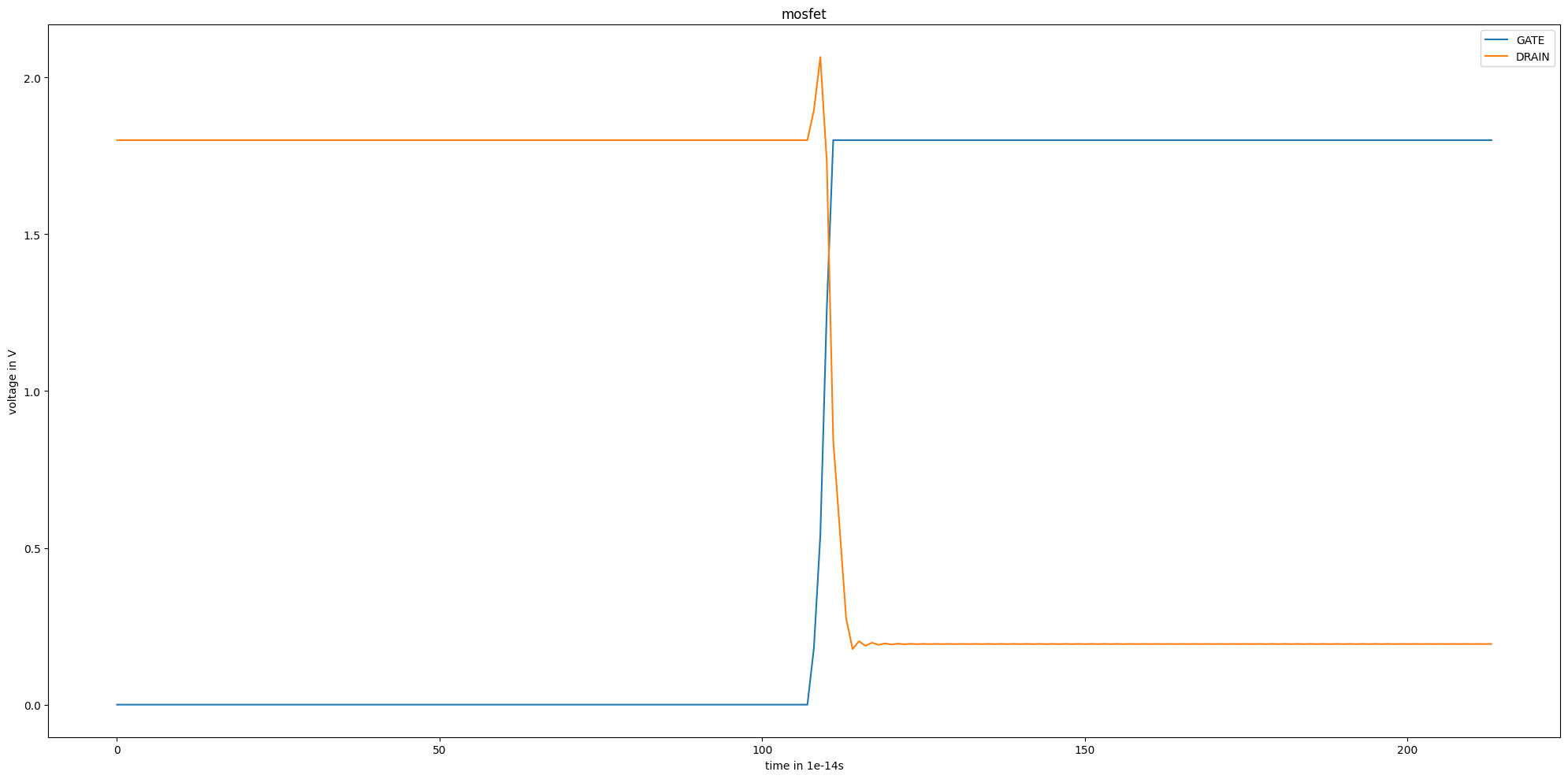
fig, ax = plt.subplots(figsize=(20, 10))
ax.set_title('mosfet')
ax.set_xlabel('time in 1e-14s')
ax.set_ylabel('voltage in V')
ax.plot(analysis.GATE)
ax.plot(analysis.DRAIN)
ax.legend(('GATE', 'DRAIN'))
plt.tight_layout()
plt.show()
1
2
3
4
5
6
7
8
9
10
.title mosfet0
.include /home/snit.san/chip_design_tape_out/analog_sim/mosfet.spice
.lib /home/snit.san/miniconda3/envs/chipReal/share/pdk/sky130A/libs.tech/ngspice/sky130.lib.spice tt
Xmosfet0 DRAIN GATE VGND mosfet
Vgnd VGND 0 0
Vdd VPWR VGND 1.8
R VPWR DRAIN 10k
VVin GATE VGND DC 0V PULSE(0V 1.8V 1ns 10ps 10ps 1ns 2ns)

done
References/Sources:
- Digital inverter with OpenLane https://developers.google.com/silicon/guides/digital-inverter-openlane